
Reports
Reports
Companies in the thin wafers market are ensuring that vendors and supply chain partners have business continuity plans in place during the ongoing COVID-19 outbreak. A severe shortage of chips is witnessed in the automotive industry, as manufacturing facilities are either shutdown or functioning at low capacities. Nevertheless, manufacturers are taking advantage of mass inoculation measures that are helping to improve market sentiments.
Companies in the thin wafers market are implementing technology upgrades such as collaboration, cloud, and automation technologies. The pandemic is anticipated to draw a positive impact on investments in the adoption of 5G, the IoT (Internet of Things), and artificial intelligence (AI). Manufacturers are entering the plug and play mode to adjust with volatile demand sentiments.
Thin wafers hold potentials in solar cells to achieve light trapping. These wafers are typically 2-10um pyramidal structures etched into the cell’s surface. Light trapping has long been achieved for thin film cells by forming wavelength-scale texturing on a substrate and then subsequently depositing the thin-film cell. However, this substrate-texturing approach has become problematic as cells are made thinner in an effort to save absorber material cost, but it affects cell morphology and back surface recombination. In order to overcome this issue, companies are increasing R&D in nanotechnology to enable light management in solar cells.
Nanotechnology is giving rise to photonic structures and plasmonics that help to improve cell performance.
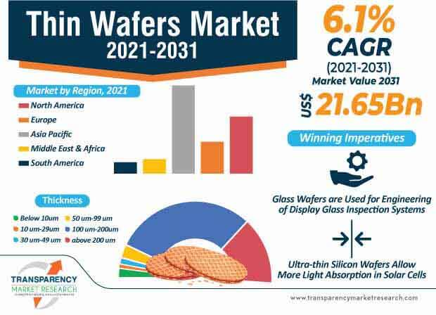
Despite restraints in solar cell designs, companies in the thin wafers market are tapping revenue opportunities in solar panels with the help of ultra-thin silicon wafers. Thinner wafers allow more light to be absorbed, so less silicon is needed to make the same amount of electricity. Moreover, thinner wafers are easier to make, so they cost less and take less time to make. Cost efficiency attributes of thinner wafers are preferred by manufacturers and end users, since the electricity they make is cheaper.
Manufacturers in the thin wafers market are boosting output capacities in ultra-thin wafers, since they have the potential to reduce the cost of fabricating solar panels.
The thin wafers market is predicted to reach US$ 21.65 Bn in 2031. Apart from silicon or gallium arsenide (GaAs), manufacturers are innovating in glass wafers to broaden their income sources. Glass wafers are thin discs of precision glass used as a substrate carrier for bonding silicon and other substrates for MEMs (Micro Electro Mechanical Systems).
Manufacturers in the thin wafers market are increasing production capabilities in glass wafers, as they are used for engineering of displays and display glass inspection systems. Low electrical loss is a prime advantage of glass wafers.
The thin wafers market is projected to expand at a favorable CAGR of 6.1% during the forecast period. Optical semiconductors are generating incremental opportunities for market stakeholders. A multi-step sequence is carried out to create the desired semiconductor devices. In front-end process, wafers are engineered and in the back-end process, they are separated into individual elements or chips and later the qualified chips are assembled into packages.
Companies in the thin wafers market monitor each stage of serial processes and sampling. Total inspection is conducted in accordance with procedures to administrate and control the processes & quality for an ultimate guarantee of quality. Wafer inspection is gaining importance as electrical performance is proved on a test machine. All of the individual elements connected on a wafer are subjected to such an electrical test for functional imperfections and are determined as good with meeting the requested specifications. Thus, optical semiconductor devices are subject to a variety of qualification tests.
Analysts’ Viewpoint
Manufacturers in the thin wafers market are revising their business continuity plans in order to keep economies running during the ongoing COVID-19 outbreak. Since substrate-texturing approach in solar cells is becoming problematic as thin wafers affect cell morphology and back surface recombination, companies should increase R&D in nanotechnology to improve cell performance. In order to provide a more flexible substrate for the production of ultra-thin semiconductors, manufacturers should produce thicker silicon rings to support ultrasonic wafers. They should also unlock value-grab opportunities in glass wafers, as they offer better warp management i.e. thermal expansion and increased stiffness helps to minimize warping. Glass wafers have the potential to deploy cost efficient processes for MEMs.
| Attribute | Detail |
|---|---|
| Market Size Value in 2020 (Base Year) | US$ 11.31 Bn |
| Market Forecast Value in 2031 | US$ 21.65 Bn |
| Growth Rate (CAGR) | 6.1% |
| Forecast Period | 2021-2031 |
| Quantitative Units | US$ Bn for Value & Units for Volume |
| Market analysis | It includes cross segment analysis at global as well as regional level. Further, qualitative analysis includes drivers, restraints, opportunities, key trends, porters five forces analysis, supply chain analysis, parent industry overview, etc. |
| Competition Landscape |
|
| Format | Electronic (PDF) or word + Excel |
| Regions Covered |
|
| Countries Covered |
|
| Market Segmentation |
|
| Companies Profiled |
|
| Customization Scope | Available upon Request |
| Pricing | Available upon Request |
Thin Wafers Market To Reach Valuation Of US$ 21.65 Bn By 2031.
Global thin wafers market is estimated to expand at a CAGR of 6.1% during the forecast period.
Power devices and CMOS image sensors are driving the thin wafers market. Thin wafer offers very thin packaging and consequently, better form factor, improved electrical performance, and high heat dissipation. Wafer level packaging in power MOSFETs, power management ICs, controllers, battery management devices, CMOS image sensors, DC converters, and some memory devices is driving the demand for thin wafers.
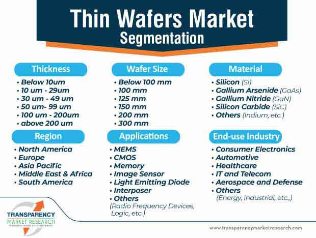
Global thin wafer market is segmented on the basis of Type, Application, Vertical, and Geography.
Key players operating in the global thin wafers market include SUMCO CORPORATION, Siltronic AG, SK Siltron Co. Ltd., Global Wafers Co. Ltd., Shin-Etsu Chemical Co., Ltd., Okmetic, Soitec, and Hangzhou Semiconductor Wafer Co., Ltd.
1. Preface
1.1. Market Introduction
1.2. Market and Segments Definition
1.3. Market Taxonomy
1.4. Research Methodology
1.5. Assumption and Acronyms
2. Executive Summary
2.1. Global Thin Wafers Market Analysis and Forecast
2.2. Regional Outline
2.3. Market Dynamics Snapshot
2.4. Competition Blueprint
3. Market Dynamics
3.1. Macro-economic Factors
3.2. Key Market Indicator
3.3. Drivers
3.4. Economic Drivers
3.4.1. Supply Side Drivers
3.4.2. Demand Side Drivers
3.5. Market Restraints and Opportunities
3.6. Market Trends
3.6.1. Demand Side
3.6.2. Supply Side
3.7. Regulatory Framework
4. Associated Industry and Key Indicator Assessment
4.1. Parent Industry Overview - Electronic Components
4.2. Supply Chain Analysis
4.3. Wafer Size Roadmap Analysis
4.4. Industry SWOT Analysis
4.5. Porter Five Forces Analysis
4.6. COVID 19 Impact Analysis
5. Global Thin Wafers Market Analysis, by Thickness
5.1. Global Thin Wafers Market Size (US$ Mn) Analysis & Forecast, by Thickness, 2017-2031
5.1.1. Below 10 um
5.1.2. 10 um -50 um
5.1.3. 50um -100 um
5.1.4. 100um-150 um
5.1.5. 150um-200 um
5.1.6. Above 200 um
5.2. Global Thin Wafers Market Attractiveness Analysis, by Thickness
6. Global Thin Wafers Market Analysis, by Wafer Size
6.1. Global Thin Wafers Market Size (US$ Mn) Analysis & Forecast, by Wafer Size, 2017-2031
6.1.1. Below 100 mm
6.1.2. 100 mm
6.1.3. 125 mm
6.1.4. 150 mm
6.1.5. 200 mm
6.1.6. 300 mm
6.2. Global Thin Wafers Market Attractiveness Analysis, by Wafer Size
7. Global Thin Wafers Market Analysis, by Material
7.1. Global Thin Wafers Market Size (US$ Mn) Analysis & Forecast, by Material, 2017-2031
7.1.1. Silicon (Si)
7.1.2. Gallium Arsenide (GaAs)
7.1.3. Gallium nitride (GaN)
7.1.4. Silicon carbide (SiC)
7.1.5. Others (Indium, Silicon carbide, etc.)
7.2. Global Thin Wafers Market Attractiveness Analysis, by Material
8. Global Thin Wafers Market Analysis, by Application
8.1. Global Thin Wafers Market Size (US$ Mn) Analysis & Forecast, by Application, 2017-2031
8.1.1. MEMS
8.1.2. CMOS
8.1.3. Memory
8.1.4. Image Sensor
8.1.5. Light Emitting Diode
8.1.6. Interposer
8.1.7. Others (radio frequency devices, logic, etc.)
8.2. Global Thin Wafers Market Attractiveness Analysis, by Application
9. Global Thin Wafers Market Analysis, by End-use Industry
9.1. Global Thin Wafers Market Size (US$ Mn) Analysis & Forecast, by End-use Industry, 2017-2031
9.1.1. Consumer Electronics
9.1.2. Automotive
9.1.3. Healthcare
9.1.4. IT and Telecom
9.1.5. Aerospace and Defense
9.1.6. Others (Energy, industrial, etc.,)
9.2. Global Thin Wafers Market Attractiveness Analysis, by End-use Industry
10. Global Thin Wafers Market Analysis and Forecast, by Region
10.1. Global Thin Wafers Market Size (US$ Mn) Analysis & Forecast, by Region, 2017-2031
10.1.1. North America
10.1.2. Europe
10.1.3. Asia Pacific
10.1.4. Middle East & Africa
10.1.5. South America
10.2. Global Thin Wafers Market Attractiveness Analysis, by Region
11. North America Thin Wafers Market Analysis and Forecast
11.1. Market Snapshot
11.2. Key Trends Analysis
11.3. Drivers and Restraints: Impact Analysis
11.4. Pricing Analysis
11.5. Key Regulations
11.6. North America Thin Wafers Market Size (US$ Mn) Analysis & Forecast, by Thickness, 2017-2031
11.6.1. Below 10 um
11.6.2. 10 um -50 um
11.6.3. 50um -100 um
11.6.4. 100um-150 um
11.6.5. 150um-200 um
11.6.6. Above 200 um
11.7. North America Thin Wafers Market Size (US$ Mn) Analysis & Forecast, by Wafer Size, 2017-2031
11.7.1. Below 100 mm
11.7.2. 100 mm
11.7.3. 125 mm
11.7.4. 150 mm
11.7.5. 200 mm
11.7.6. 300 mm
11.8. North America Thin Wafers Market Size (US$ Mn) Analysis & Forecast, by Material, 2017-2031
11.8.1. Silicon (Si)
11.8.2. Gallium Arsenide (GaAs)
11.8.3. Gallium nitride (GaN)
11.8.4. Silicon carbide (SiC)
11.8.5. Others (Indium, Silicon carbide, etc.)
11.9. North America Thin Wafers Market Size (US$ Mn) Analysis & Forecast, by Application, 2017-2031
11.9.1. MEMS
11.9.2. CMOS
11.9.3. Memory
11.9.4. Image Sensor
11.9.5. Light Emitting Diode
11.9.6. Interposer
11.9.7. Others (radio frequency devices, logic, etc.)
11.10. North America Thin Wafers Market Size (US$ Mn) Analysis & Forecast, by End-use Industry, 2017-2031
11.10.1. Consumer Electronics
11.10.2. Automotive
11.10.3. Healthcare
11.10.4. IT and Telecom
11.10.5. Aerospace and Defense
11.10.6. Others (Energy, industrial, etc.,)
11.11. North America Thin Wafers Market Size (US$ Mn) Analysis & Forecast, by Country, 2017-2031
11.11.1. U.S.
11.11.2. Canada
11.11.3. Rest of North America
11.12. North America Thin Wafers Market Attractiveness Analysis
11.12.1. By Thickness
11.12.2. By Wafer Size
11.12.3. By Application
11.12.4. By End-use Industry
11.12.5. By Country
12. Europe Thin Wafers Market Analysis and Forecast
12.1. Market Snapshot
12.2. Key Trends Analysis
12.3. Drivers and Restraints: Impact Analysis
12.4. Pricing Analysis
12.5. Key Regulations
12.6. Europe Thin Wafers Market Size (US$ Mn) Analysis & Forecast, by Thickness, 2017-2031
12.6.1. Below 10 um
12.6.2. 10 um -50 um
12.6.3. 50um -100 um
12.6.4. 100um-150 um
12.6.5. 150um-200 um
12.6.6. Above 200 um
12.7. Europe Thin Wafers Market Size (US$ Mn) Analysis & Forecast, by Wafer Size, 2017-2031
12.7.1. Below 100 mm
12.7.2. 100 mm
12.7.3. 125 mm
12.7.4. 150 mm
12.7.5. 200 mm
12.7.6. 300 mm
12.8. Europe Thin Wafers Market Size (US$ Mn) Analysis & Forecast, by Material, 2017-2031
12.8.1. Silicon (Si)
12.8.2. Gallium Arsenide (GaAs)
12.8.3. Gallium nitride (GaN)
12.8.4. Silicon carbide (SiC)
12.8.5. Others (Indium, Silicon carbide, etc.)
12.9. Europe Thin Wafers Market Size (US$ Mn) Analysis & Forecast, by Application, 2017-2031
12.9.1. MEMS
12.9.2. CMOS
12.9.3. Memory
12.9.4. Image Sensor
12.9.5. Light Emitting Diode
12.9.6. Interposer
12.9.7. Others (radio frequency devices, logic, etc.)
12.10. Europe Thin Wafers Market Size (US$ Mn) Analysis & Forecast, by End-use Industry, 2017-2031
12.10.1. Consumer Electronics
12.10.2. Automotive
12.10.3. Healthcare
12.10.4. IT and Telecom
12.10.5. Aerospace and Defense
12.10.6. Others (Energy, industrial, etc.,)
12.11. Europe Thin Wafers Market Size (US$ Mn) Analysis & Forecast, by Country & Sub-region, 2017-2031
12.11.1. U.K.
12.11.2. Germany
12.11.3. France
12.11.4. Italy
12.11.5. Russia
12.11.6. Rest of Europe
12.12. Europe Thin Wafers Market Attractiveness Analysis
12.12.1. By Thickness
12.12.2. By Wafer Size
12.12.3. By Application
12.12.4. By End-use Industry
12.12.5. By Country & Sub-region
13. Asia Pacific Thin Wafers Market Analysis and Forecast
13.1. Market Snapshot
13.2. Key Trends Analysis
13.3. Drivers and Restraints: Impact Analysis
13.4. Pricing Analysis
13.5. Key Regulations
13.6. Asia Pacific Thin Wafers Market Size (US$ Mn) Analysis & Forecast, by Thickness, 2017-2031
13.6.1. Below 10 um
13.6.2. 10 um -50 um
13.6.3. 50um -100 um
13.6.4. 100um-150 um
13.6.5. 150um-200 um
13.6.6. Above 200 um
13.7. Asia Pacific Thin Wafers Market Size (US$ Mn) Analysis & Forecast, by Wafer Size, 2017-2031
13.7.1. Below 100 mm
13.7.2. 100 mm
13.7.3. 125 mm
13.7.4. 150 mm
13.7.5. 200 mm
13.7.6. 300 mm
13.8. Asia Pacific Thin Wafers Market Size (US$ Mn) Analysis & Forecast, by Material, 2017-2031
13.8.1. Silicon (Si)
13.8.2. Gallium Arsenide (GaAs)
13.8.3. Gallium nitride (GaN)
13.8.4. Silicon carbide (SiC)
13.8.5. Others (Indium, Silicon carbide, etc.)
13.9. Asia Pacific Thin Wafers Market Size (US$ Mn) Analysis & Forecast, by Application, 2017-2031
13.9.1. MEMS
13.9.2. CMOS
13.9.3. Memory
13.9.4. Image Sensor
13.9.5. Light Emitting Diode
13.9.6. Interposer
13.9.7. Others (radio frequency devices, logic, etc.)
13.10. Asia Pacific Thin Wafers Market Size (US$ Mn) Analysis & Forecast, by End-use Industry, 2017-2031
13.10.1. Consumer Electronics
13.10.2. Automotive
13.10.3. Healthcare
13.10.4. IT and Telecom
13.10.5. Aerospace and Defense
13.10.6. Others (Energy, industrial, etc.,)
13.11. Asia Pacific Thin Wafers Market Size (US$ Mn) Analysis & Forecast, by Country & Sub-region, 2017-2031
13.11.1. China
13.11.2. India
13.11.3. Japan
13.11.4. South Korea
13.11.5. ASEAN
13.11.6. Rest of Asia Pacific
13.12. Asia Pacific Thin Wafers Market Attractiveness Analysis
13.12.1. By Thickness
13.12.2. By Wafer Size
13.12.3. By Application
13.12.4. By End-use Industry
13.12.5. By Country & Sub-region
14. Middle East & Africa (MEA) Thin Wafers Market Analysis and Forecast
14.1. Market Snapshot
14.2. Key Trends Analysis
14.3. Drivers and Restraints: Impact Analysis
14.4. Pricing Analysis
14.5. Key Regulations
14.6. Middle East & Africa Thin Wafers Market Size (US$ Mn) Analysis & Forecast, by Thickness, 2017-2031
14.6.1. Below 10 um
14.6.2. 10 um -50 um
14.6.3. 50um -100 um
14.6.4. 100um-150 um
14.6.5. 150um-200 um
14.6.6. Above 200 um
14.7. Middle East & Africa Thin Wafers Market Size (US$ Mn) Analysis & Forecast, by Wafer Size, 2017-2031
14.7.1. Below 100 mm
14.7.2. 100 mm
14.7.3. 125 mm
14.7.4. 150 mm
14.7.5. 200 mm
14.7.6. 300 mm
14.8. Middle East & Africa Thin Wafers Market Size (US$ Mn) Analysis & Forecast, by Material, 2017-2031
14.8.1. Silicon (Si)
14.8.2. Gallium Arsenide (GaAs)
14.8.3. Gallium nitride (GaN)
14.8.4. Silicon carbide (SiC)
14.8.5. Others (Indium, Silicon carbide, etc.)
14.9. Middle East & Africa Thin Wafers Market Size (US$ Mn) Analysis & Forecast, by Application, 2017-2031
14.9.1. MEMS
14.9.2. CMOS
14.9.3. Memory
14.9.4. Image Sensor
14.9.5. Light Emitting Diode
14.9.6. Interposer
14.9.7. Others (radio frequency devices, logic, etc.)
14.10. Middle East & Africa Thin Wafers Market Size (US$ Mn) Analysis & Forecast, by End-use Industry, 2017-2031
14.10.1. Consumer Electronics
14.10.2. Automotive
14.10.3. Healthcare
14.10.4. IT and Telecom
14.10.5. Aerospace and Defense
14.10.6. Others (Energy, industrial, etc.,)
14.11. Middle East & Africa Thin Wafers Market Size (US$ Mn) Analysis & Forecast, by Country & Sub-region, 2017-2031
14.11.1. GCC
14.11.2. South Africa
14.11.3. North Africa
14.11.4. Rest of Middle East & Africa
14.12. Middle East & Africa Thin Wafers Market Attractiveness Analysis
14.12.1. By Thickness
14.12.2. By Wafer Size
14.12.3. By Application
14.12.4. By End-use Industry
14.12.5. By Country & Sub-region
15. South America Thin Wafers Market Analysis and Forecast
15.1. Market Snapshot
15.2. Key Trends Analysis
15.3. Drivers and Restraints: Impact Analysis
15.4. Pricing Analysis
15.5. Key Regulations
15.6. South America Thin Wafers Market Size (US$ Mn) Analysis & Forecast, by Thickness, 2017-2031
15.6.1. Below 10 um
15.6.2. 10 um -50 um
15.6.3. 50um -100 um
15.6.4. 100um-150 um
15.6.5. 150um-200 um
15.6.6. Above 200 um
15.7. South America Thin Wafers Market Size (US$ Mn) Analysis & Forecast, by Wafer Size, 2017-2031
15.7.1. Below 100 mm
15.7.2. 100 mm
15.7.3. 125 mm
15.7.4. 150 mm
15.7.5. 200 mm
15.7.6. 300 mm
15.8. South America Thin Wafers Market Size (US$ Mn) Analysis & Forecast, by Material, 2017-2031
15.8.1. Silicon (Si)
15.8.2. Gallium Arsenide (GaAs)
15.8.3. Gallium nitride (GaN)
15.8.4. Silicon carbide (SiC)
15.8.5. Others (Indium, Silicon carbide, etc.)
15.9. South America Thin Wafers Market Size (US$ Mn) Analysis & Forecast, by Application, 2017-2031
15.9.1. MEMS
15.9.2. CMOS
15.9.3. Memory
15.9.4. Image Sensor
15.9.5. Light Emitting Diode
15.9.6. Interposer
15.9.7. Others (radio frequency devices, logic, etc.)
15.10. South America Thin Wafers Market Size (US$ Mn) Analysis & Forecast, by Country & Sub-region, 2017-2031
15.10.1. Brazil
15.10.2. Argentina
15.10.3. Rest of South America
15.11. South America Thin Wafers Market Attractiveness Analysis
15.11.1. By Thickness
15.11.2. By Wafer Size
15.11.3. By Application
15.11.4. By End-use Industry
15.11.5. By Country & Sub-region
16. Competition Assessment
16.1. Global Thin Wafers Market Competition Matrix - a Dashboard View
16.1.1. Global Thin Wafers Market Company Share Analysis, by Value (2020) and Volume
16.1.2. Technological Differentiator
17. Company Profiles (Manufacturers/Suppliers)
17.1. SUMCO CORPORATION
17.1.1. Overview
17.1.2. Product Portfolio
17.1.3. Sales Footprint
17.1.4. Key Subsidiaries or Distributors
17.1.5. Strategy and Recent Developments
17.1.6. Financial Analysis
17.2. Siltronic AG
17.2.1. Overview
17.2.2. Product Portfolio
17.2.3. Sales Footprint
17.2.4. Key Subsidiaries or Distributors
17.2.5. Strategy and Recent Developments
17.2.6. Financial Analysis
17.3. SK Siltron Co.,Ltd
17.3.1. Overview
17.3.2. Product Portfolio
17.3.3. Sales Footprint
17.3.4. Key Subsidiaries or Distributors
17.3.5. Strategy and Recent Developments
17.3.6. Financial Analysis
17.4. GlobalWafers Co., Ltd (Universal Wafer Co., Ltd.)
17.4.1. Overview
17.4.2. Product Portfolio
17.4.3. Sales Footprint
17.4.4. Key Subsidiaries or Distributors
17.4.5. Strategy and Recent Developments
17.4.6. Financial Analysis
17.5. Shin-Etsu Chemical Co., Ltd.
17.5.1. Overview
17.5.2. Product Portfolio
17.5.3. Sales Footprint
17.5.4. Key Subsidiaries or Distributors
17.5.5. Strategy and Recent Developments
17.5.6. Financial Analysis
17.6. Okmetic
17.6.1. Overview
17.6.2. Product Portfolio
17.6.3. Sales Footprint
17.6.4. Key Subsidiaries or Distributors
17.6.5. Strategy and Recent Developments
17.6.6. Financial Analysis
17.7. Hangzhou Semiconductor Wafer Co., Ltd.
17.7.1. Overview
17.7.2. Product Portfolio
17.7.3. Sales Footprint
17.7.4. Key Subsidiaries or Distributors
17.7.5. Strategy and Recent Developments
17.7.6. Financial Analysis
17.8. SOITEC
17.8.1. Overview
17.8.2. Product Portfolio
17.8.3. Sales Footprint
17.8.4. Key Subsidiaries or Distributors
17.8.5. Strategy and Recent Developments
17.8.6. Financial Analysis
18. Recommendation
18.1. Opportunity Assessment
18.1.1. By Thickness
18.1.2. By Wafer Size
18.1.3. By Application
18.1.4. By End-use Industry
18.1.5. By Region
List of Tables
Table 01: Global Thin Wafers Market Value (US$ Mn) Forecast, by Thickness, 2017-2031
Table 02: Global Thin Wafers Market Value (US$ Mn) Forecast, by Wafer Size, 2017-2031
Table 03: Global Thin Wafers Market Value (US$ Mn) Forecast, by Material, 2017-2031
Table 04: Global Thin Wafers Market Value (US$ Mn) Forecast, by Application, 2017-2031
Table 05: Global Thin Wafers Market Value (US$ Mn) Forecast, by End-use Industry, 2017-2031
Table 06: Global Thin Wafers Market Value (US$ Mn) Forecast, by Region, 2017-2031
Table 07: North America Thin Wafers Market Value (US$ Mn) Forecast, by Thickness, 2017-2031
Table 08: North America Thin Wafers Market Value (US$ Mn) Forecast, by Wafer Size, 2017-2031
Table 09: North America Thin Wafers Market Value (US$ Mn) Forecast, by Material, 2017-2031
Table 10: North America Thin Wafers Market Value (US$ Mn) Forecast, by Application, 2017-2031
Table 11: North America Thin Wafers Market Value (US$ Mn) Forecast, by End-use Industry, 2017-2031
Table 12: North America Thin Wafers Market Value (US$ Mn) Forecast, by Country, 2017-2031
Table 14: Europe Thin Wafers Market Value (US$ Mn) Forecast, by Wafer Size, 2017-2031
Table 15: Europe Thin Wafers Market Value (US$ Mn) Forecast, by Material, 2017-2031
Table 16: Europe Thin Wafers Market Value (US$ Mn) Forecast, by Application, 2017-2031
Table 17: Europe Thin Wafers Market Value (US$ Mn) Forecast, by End-use Industry, 2017-2031
Table 18: Europe Thin Wafers Market Value (US$ Mn) Forecast, by Country & Sub-region, 2017-2031
Table 19: Asia Pacific Thin Wafers Market Value (US$ Mn) Forecast, by Thickness, 2017-2031
Table 20: Asia Pacific Thin Wafers Market Value (US$ Mn) Forecast, by Wafer Size, 2017-2031
Table 21: Asia Pacific Thin Wafers Market Value (US$ Mn) Forecast, by Material, 2017-2031
Table 22: Asia Pacific Thin Wafers Market Value (US$ Mn) Forecast, by Application, 2017-2031
Table 23: Asia Pacific Thin Wafers Market Value (US$ Mn) Forecast, by End-use Industry, 2017-2031
Table 24: Asia Pacific Thin Wafers Market Value (US$ Mn) Forecast, by Country & Sub-region, 2017-2031
Table 25: Middle East & Africa Thin Wafers Market Value (US$ Mn) Forecast, by Thickness, 2017-2031
Table 26: Middle East & Africa Thin Wafers Market Value (US$ Mn) Forecast, by Wafer Size, 2017-2031
Table 27: Middle East & Africa Thin Wafers Market Value (US$ Mn) Forecast, by Material, 2017-2031
Table 28: Middle East & Africa Thin Wafers Market Value (US$ Mn) Forecast, by Application, 2017-2031
Table 29: Middle East & Africa Thin Wafers Market Value (US$ Mn) Forecast, by End-use Industry, 2017-2031
Table 30: Middle East & Africa Thin Wafers Market Value (US$ Mn) Forecast, by Country & Sub-region, 2017-2031
Table 31: South America Thin Wafers Market Value (US$ Mn) Forecast, by Thickness, 2017-2031
Table 32: South America Thin Wafers Market Value (US$ Mn) Forecast, by Wafer Size, 2017-2031
Table 33: South America Thin Wafers Market Value (US$ Mn) Forecast, by Material, 2017-2031
Table 34: South America Thin Wafers Market Value (US$ Mn) Forecast, by Application, 2017-2031
Table 35: South America Thin Wafers Market Value (US$ Mn) Forecast, by End-use Industry, 2017-2031
Table 36: South America Thin Wafers Market Value (US$ Mn) Forecast, by Country & Sub-region, 2017-2031
List of Figures
Figure 01: Global Thin Wafer Market, Value (US$ Mn), 2017-2031
Figure 02: Global Thin Wafers Market, Value (US$ Mn), 2017-2031
Figure 03: Global Thin Wafers Market Size & Forecast, by Thickness, Revenue (US$ Mn), 2017-2031
Figure 04: Global Thin Wafers Market Attractiveness, by Thickness, 2021-2031
Figure 05: Global Thin Wafers Market Share Analysis, by Diamond Thickness, 2021 and 2031
Figure 06: Global Thin Wafers Market Size & Forecast, by Wafer Size, Revenue (US$ Mn), 2017-2031
Figure 07: Global Thin Wafers Market Attractiveness, by Wafer Size, 2021-2031
Figure 08: Global Thin Wafers Market Share Analysis, by Wafer Size, 2021 and 2031
Figure 09: Global Thin Wafers Market Size & Forecast, by Material, Revenue (US$ Mn), 2017-2031
Figure 10: Global Thin Wafers Market Attractiveness, by Material, 2021-2031
Figure 11: Global Thin Wafers Market Share Analysis, by Material, 2021 and 2031
Figure 12: Global Thin Wafers Market Size & Forecast, by Application, Revenue (US$ Mn), 2017-2031
Figure 13: Global Thin Wafers Market Attractiveness, by Application, 2021-2031
Figure 14: Global Thin Wafers Market Share Analysis, by Application, 2021 and 2031
Figure 15: Global Thin Wafers Market Size & Forecast, by End-use Industry, Revenue (US$ Mn), 2017-2031
Figure 16: Global Thin Wafers Market Attractiveness, by End-use Industry, 2021-2031
Figure 17: Global Thin Wafers Market Share Analysis, by End-use Industry, 2021 and 2031
Figure 18: Global Thin Wafers Market Size & Forecast, by Region, Revenue (US$ Mn), 2017-2031
Figure 19: Global Thin Wafers Market Attractiveness, by Region, 2021-2031
Figure 20: Global Thin Wafers Market Share Analysis, by Region, 2021 and 2031
Figure 21: North America Thin Wafers Market, Value (US$ Mn), 2017-2031
Figure 22: North America Thin Wafers Market, Value (US$ Mn), 2017-2031 (Y-o-Y Growth)
Figure 23: North America Thin Wafers Market Size & Forecast, by Thickness, Revenue (US$ Mn), 2017-2031
Figure 24: North America Thin Wafers Market Attractiveness, by Thickness, 2021-2031
Figure 25: North America Thin Wafers Market Share Analysis, by Thickness, 2021 and 2031
Figure 26: North America Thin Wafers Market Size & Forecast, by Wafer Size, Revenue (US$ Mn), 2017-2031
Figure 27: North America Thin Wafers Market Attractiveness, by Wafer Size, 2021-2031
Figure 28: North America Thin Wafers Market Share Analysis, by Wafer Size, 2021 and 2031
Figure 29: North America Thin Wafers Market Size & Forecast, by Material, Revenue (US$ Mn), 2017-2031
Figure 30: North America Thin Wafers Market Attractiveness, by Material, Value (US$ Mn), 2021-2031
Figure 31: North America Thin Wafers Market Share Analysis, by Material, 2021 and 2031
Figure 32: North America Thin Wafers Market Size & Forecast, by Application, Revenue (US$ Mn), 2017-2031
Figure 32: North America Thin Wafers Market Attractiveness, by Application, 2021-2031
Figure 33: North America Thin Wafers Market Attractiveness, by Application, 2021-2031
Figure 34: North America Thin Wafers Market Share Analysis, by Application, 2021 and 2031
Figure 35: North America Thin Wafers Market Size & Forecast, by End-use Industry, Revenue (US$ Mn), 2017-2031
Figure 36: North America Thin Wafers Market Attractiveness, by End-use Industry, 2021-2031
Figure 37: North America Thin Wafers Market Share Analysis, by End-use Industry, 2021 and 2031
Figure 38: North America Thin Wafers Market Size & Forecast, by Country, Revenue (US$ Mn), 2017-2031
Figure 39: North America Thin Wafers Market Attractiveness, by Country, 2021-2031
Figure 40: North America Thin Wafers Market Share Analysis, by Country, 2021 and 2031
Figure 41: Europe Thin Wafers Market, Value (US$ Mn), 2017-2031
Figure 42: Europe Thin Wafers Market, Value (US$ Mn), 2017-2031 (Y-o-Y Growth)
Figure 43: Europe Thin Wafers Market Size & Forecast, by Thickness, Revenue (US$ Mn), 2017-2031
Figure 44: Europe Thin Wafers Market Attractiveness, by Thickness, 2021-2031
Figure 45: Europe Thin Wafers Market Share Analysis, by Thickness, 2021 and 2031
Figure 46: Europe Thin Wafers Market Size & Forecast, by Wafer Size, Revenue (US$ Mn), 2017-2031
Figure 47: Europe Thin Wafers Market Attractiveness, by Wafer Size, 2021-2031
Figure 48: Europe Thin Wafers Market Share Analysis, by Wafer Size, 2021 and 2031
Figure 49: Europe Thin Wafers Market Size & Forecast, by Material, Revenue (US$ Mn), 2017-2031
Figure 50: Europe Thin Wafers Market Attractiveness, by Material, Value (US$ Mn), 2021-2031
Figure 51: Europe Thin Wafers Market Share Analysis, by Material, 2021 and 2031
Figure 52: Europe Thin Wafers Market Size & Forecast, by Application, Revenue (US$ Mn), 2017-2031
Figure 53: Europe Thin Wafers Market Attractiveness, by Application, 2021-2031
Figure 54: Europe Thin Wafers Market Share Analysis, by Application, 2021 and 2031
Figure 55: Europe Thin Wafers Market Size & Forecast, by End-use Industry, Revenue (US$ Mn), 2017-2031
Figure 56: Europe Thin Wafers Market Attractiveness, by End-use Industry, 2021-2031
Figure 57: Europe Thin Wafers Market Share Analysis, by End-use Industry, 2021 and 2031
Figure 58: Europe Thin Wafers Market Size & Forecast, by Country & Sub-region, Revenue (US$ Mn), 2017-2031
Figure 59: Europe Thin Wafers Market Attractiveness, by Country & Sub-region, 2021-2031
Figure 60: Europe Thin Wafers Market Share Analysis, by Country & Sub-region, 2021 and 2031
Figure 61: Asia Pacific Thin Wafers Market, Value (US$ Mn), 2017-2031
Figure 62: Asia Pacific Thin Wafers Market, Value (US$ Mn), 2017-2031 (Y-o-Y Growth)
Figure 63: Asia Pacific Thin Wafers Market Size & Forecast, by Thickness, Revenue (US$ Mn), 2017-2031
Figure 64: Asia Pacific Thin Wafers Market Attractiveness, by Thickness, 2021-2031
Figure 65: Asia Pacific Thin Wafers Market Share Analysis, by Thickness, 2021 and 2031
Figure 66: Asia Pacific Thin Wafers Market Size & Forecast, by Wafer Size, Revenue (US$ Mn), 2017-2031
Figure 67: Asia Pacific Thin Wafers Market Attractiveness, by Wafer Size, 2021-2031
Figure 68: Asia Pacific Thin Wafers Market Share Analysis, by Wafer Size, 2021 and 2031
Figure 69: Asia Pacific Thin Wafers Market Size & Forecast, by Material, Revenue (US$ Mn), 2017-2031
Figure 70: Asia Pacific Thin Wafers Market Attractiveness, by Material, Value (US$ Mn), 2021-2031
Figure 71: Asia Pacific Thin Wafers Market Share Analysis, by Material, 2021 and 2031
Figure 72: Asia Pacific Thin Wafers Market Size & Forecast, by Application, Revenue (US$ Mn), 2017-2031
Figure 73: Asia Pacific Thin Wafers Market Attractiveness, by Application, 2021-2031
Figure 74: Asia Pacific Thin Wafers Market Share Analysis, by Application, 2021 and 2031
Figure 75: Asia Pacific Thin Wafers Market Size & Forecast, by End-use Industry, Revenue (US$ Mn), 2017-2031
Figure 76: Asia Pacific Thin Wafers Market Attractiveness, by End-use Industry, 2021-2031
Figure 77: Asia Pacific Thin Wafers Market Share Analysis, by End-use Industry, 2021 and 2031
Figure 78: Asia Pacific Thin Wafers Market Size & Forecast, by Country & Sub-region, Revenue (US$ Mn), 2017-2031
Figure 79: Asia Pacific Thin Wafers Market Attractiveness, by Country & Sub-region, 2021-2031
Figure 80: Asia Pacific Thin Wafers Market Share Analysis, by Country & Sub-region, 2021 and 2031
Figure 81: Middle East & Africa Thin Wafers Market, Value (US$ Mn), 2017-2031
Figure 82: Middle East & Africa Thin Wafers Market, Value (US$ Mn), 2017-2031 (Y-o-Y Growth)
Figure 83: Middle East & Africa Thin Wafers Market Size & Forecast, by Thickness, Revenue (US$ Mn), 2017-2031
Figure 84: Middle East & Africa Thin Wafers Market Attractiveness, by Thickness, 2021-2031
Figure 85: Middle East & Africa Thin Wafers Market Share Analysis, by Thickness, 2021 and 2031
Figure 86: Middle East & Africa Thin Wafers Market Size & Forecast, by Wafer Size, Revenue (US$ Mn), 2017-2031
Figure 87: Middle East & Africa Thin Wafers Market Attractiveness, by Wafer Size, 2021-2031
Figure 88: Middle East & Africa Thin Wafers Market Share Analysis, by Wafer Size, 2021 and 2031
Figure 89: Middle East & Africa Thin Wafers Market Size & Forecast, by Material, Revenue (US$ Mn), 2017-2031
Figure 90: Middle East & Africa Thin Wafers Market Attractiveness, by Material, Value (US$ Mn), 2021-2031
Figure 91: Middle East & Africa Thin Wafers Market Share Analysis, by Material, 2021 and 2031
Figure 92: Middle East & Africa Thin Wafers Market Size & Forecast, by Application, Revenue (US$ Mn), 2017-2031
Figure 93: Middle East & Africa Thin Wafers Market Attractiveness, by Application, 2021-2031
Figure 94: Middle East & Africa Thin Wafers Market Share Analysis, by Application, 2021 and 2031
Figure 95: Middle East & Africa Thin Wafers Market Size & Forecast, by End-use Industry, Revenue (US$ Mn), 2017-2031
Figure 96: Middle East & Africa Thin Wafers Market Attractiveness, by End-use Industry, 2021-2031
Figure 97: Middle East & Africa Thin Wafers Market Share Analysis, by End-use Industry, 2021 and 2031
Figure 98: Middle East & Africa Thin Wafers Market Size & Forecast, by Country & Sub-region, Revenue (US$ Mn), 2017-2031
Figure 99: Middle East & Africa Thin Wafers Market Attractiveness, by Country & Sub-region, 2021-2031
Figure 100: Middle East & Africa Thin Wafers Market Share Analysis, by Country & Sub-region, 2021 and 2031
Figure 101: South America Thin Wafers Market, Value (US$ Mn), 2017-2031
Figure 102: South America Thin Wafers Market, Value (US$ Mn), 2017-2031 (Y-o-Y Growth)
Figure 103: South America Thin Wafers Market Size & Forecast, by Thickness, Revenue (US$ Mn), 2017-2031
Figure 104: South America Thin Wafers Market Attractiveness, by Thickness, 2021-2031
Figure 105: South America Thin Wafers Market Share Analysis, by Thickness, 2021 and 2031
Figure 106: South America Thin Wafers Market Size & Forecast, by Wafer Size, Revenue (US$ Mn), 2017-2031
Figure 107: South America Thin Wafers Market Attractiveness, by Wafer Size, 2021-2031
Figure 108: South America Thin Wafers Market Share Analysis, by Wafer Size, 2021 and 2031
Figure 109: South America Thin Wafers Market Size & Forecast, by Material, Revenue (US$ Mn), 2017-2031
Figure 110: South America Thin Wafers Market Attractiveness, by Material, Value (US$ Mn), 2021-2031
Figure 111: South America Thin Wafers Market Share Analysis, by Material, 2021 and 2031
Figure 112: South America Thin Wafers Market Size & Forecast, by Application, Revenue (US$ Mn), 2017-2031
Figure 113: South America Thin Wafers Market Attractiveness, by Application, 2021-2031
Figure 114: South America Thin Wafers Market Share Analysis, by Application, 2021 and 2031
Figure 115: South America Thin Wafers Market Size & Forecast, by End-use Industry, Revenue (US$ Mn), 2017-2031
Figure 116: South America Thin Wafers Market Attractiveness, by End-use Industry, 2021-2031
Figure 117: South America Thin Wafers Market Share Analysis, by End-use Industry, 2021 and 2031
Figure 118: South America Thin Wafers Market Size & Forecast, by Country & Sub-region, Revenue (US$ Mn), 2017-2031
Figure 119: South America Thin Wafers Market Attractiveness, by Country & Sub-region, 2021-2031
Figure 120: South America Thin Wafers Market Share Analysis, by Country & Sub-region, 2021 and 2031
Figure 121: Global Thin Wafers Market Share Analysis, by Company
Copyright © Transparency Market Research, Inc. All Rights reserved
Trust Online

Thin Wafers Market